Check back soon
Once posts are published, you’ll see them here.


國立成功大學材料科學及工程學系 陳嘉勻教授實驗室
聯絡方式:06-2757575 轉分機 62952 (教授辦公室) 或分機 62961 Ext:2406 (學生研究室)
E-mail:timcychen@mail.ncku.edu.tw

Nanomaterials for green-energy technologies
Our research focuses on the realization of nanostructure-based solar cells, making them cheaper and more efficient. The overall goal is to tailor material properties such as energy-harvesting, non-reflecting, self-cleaning, and capable of integrating with current manufacturing procedures for constructing the next-generation energy devices.
Organic/inorganic hybrid solar cells
Quantum dot solar cells
Room-temperature thermoelectric devices
Water splitting for hydrogen generation

Semiconductor nanodevices
Semiconductor heterostructures are an emerging class of materials that represent the attractive building blocks for many applications. Our research focuses on the controlled synthesis, fabrication and characterization of nanostructures using a simple, inexpensive and reliable method. We aim to control their size, geometry, and understand the fundamental aspects of formation mechanism, and thus the material properties, to optimize its performance.
Synaptic devices
Optoelectronics: Phototransistor, photomemory
Semiconductor materials and devices
Stability evaluation of electronic devices


Optical metamaterials
Metamaterials composed of sub-wavelength metallic structures enable to guide the propagation of electromagnetic waves better than conventional materials. Aside from being used to tune wave propagations, metamaterial resonators are extensively used to detect the local change in the refractive index in the environment of a medium. Detection is performed by localizing the electromagnetic field of incident waves that surround metamaterial structures under resonant couplings, which allows to sense the extremely low concentration of target.
Chemical/biological sensors
Materials for 6G communication
Wide band absorber
Semiconductor processing
Metal-assisted chemical etching (MaCE), a recently developed unique etching technique, allows the fabrication of extremely high aspect ratio semiconductor nanostructure arrays. We aim to study the influences of metallic catalysts, reactant concentrations, temperatures and intrinsic properties of semiconductors to build up a comprehensive three-dimensional (3D) processing capability for the advanced development of microelectronics such as CIS, 3DIC and other functional devices.
3D processing capability
Patterning and mechanism study
Heterostructure design
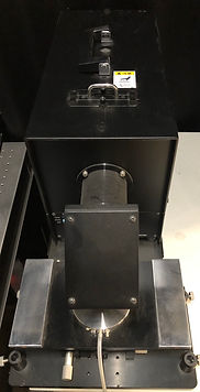
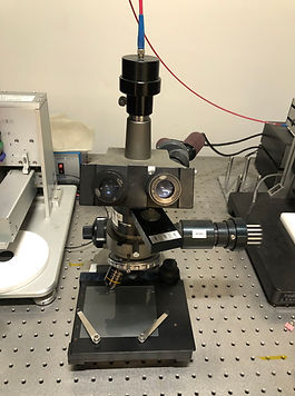
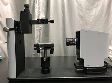
Analytic equipment
UV/Vis absorption spectrometer, Spectrophotometer, Optical microscope, Contact-angle measurement.
Simulation
Fabrication equipment
Hot plate, Furnace, Vacuum oven, Photochemical reactor, Vacuum filter, Ultrasonicator, RTA, Spin coater, Glove box.
Chemical and related equipment
Chemicals, pH meter, Centrifuge, Chemical hood.
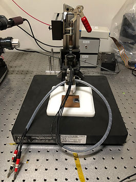
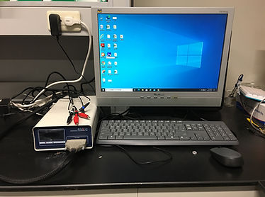
Photo/Electric/Thermal measurement
AM 1.5 solar simulator, I-V measurement system, Four-probe resistance measurement, Electrochemical workstation, PL spectrometer, Seebeck measurement, Photoresponse measurement


國立成功大學材料科學及工程學系 陳嘉勻教授實驗室
聯絡方式:06-2757575 轉分機 62952 (教授辦公室) 或分機 62961 Ext:2406 (學生研究室)
E-mail:timcychen@mail.ncku.edu.tw